When a customer orders PCBs, there are number of steps to go through before the units can be produced, from design to testing to manufacturing and everything in between. At UK Electronics, we have a reputation for quality and efficiency at every stage of the process, making us one of the most popular choices for PCB Assembly in the UK.
Each order is different and is unlikely to use an existing PCB design or layout for their unit as it might not meet their needs, especially because technology can be so different from brand to brand and device to device. That means we need to make something unique for each order and this begins with the design phase, where the PCB will be created with a schematic once we know the specific details of the order.
This includes the materials, size and its intended purpose or use in the technology you have. Once this has been completed, we can move on to the next stage and progress with your order. In some cases, we can take existing designs from other sources and check to make sure they’re suitable for your needs while in others, we’re used just to design and/or test units from other suppliers. This helps you get the best information.
Schematic before design
The schematic is a technical drawing that identifies the different parts of each PCB, where they are located and how it connects together. It’s the first stage of PCB design and is usually a 2D image that can be used as a map or guide for the next stage. This comes in the form of a 3D image or model that tests how everything will look and ensures the PCBs will meet all specifications, from size to materials to usage. In some cases, there will be multiple versions of both the schematic and the design to make sure nothing is overlooked and that the final result, when printed, will work as intended during the testing stage.
Putting it all together
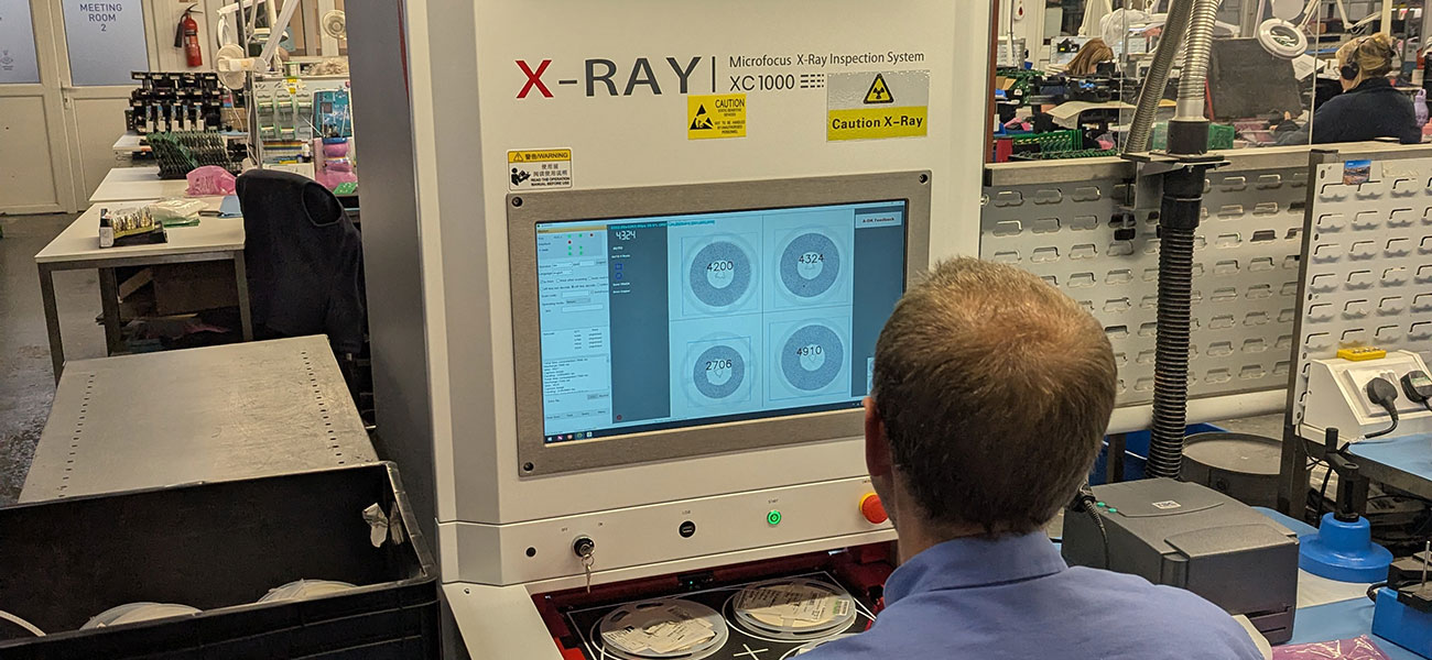
To create a fully functional PCB, both the schematic and design have to be accurate before moving onto the PCB prototyping stage. This is when we can test the unit to make sure that it works and performs as intended. Should any issues or irregularities appear, they can be fixed by going back to the schematic and design to identify the issue and make changes to correct it.
This quality control stage ensures that when PCB manufacturing starts, all units are of the highest quality and will meet all requirements you have. We’re committed to producing the highest-quality PCBs at all times, and we also use PCB prototyping to test new designs and ideas to improve the units we can provide our customers. With technology and devices changing so often, PCBs have to do the same. There are increasingly complicated designs to make sure it does everything needed for each piece of technology they’re being used for.
To find out more about PCB design, manufacturing and prototyping, get in touch with the team at UK Electronics today and see how we can help.



 PCB Design
  Electronic Assembly
  PCB Prototyping
  EMC Testing
  Box Build
  Cable Assembly